LLMs and AI copilots are entering chip design flows fast. But without the right guardrails, they introduce new classes of risk — wrong RTL, hallucinated...
TSMC unveiled A13/A12/N2U nodes. AI dethroned smartphones as TSMC top revenue driver. Foundry capacity wars locked out smaller players. Agentic EDA went mainstream. Here are...
Why Design for Testability Matters Design for Testability (DFT) is a critical discipline in modern chip design. Without DFT, manufactured chips cannot be efficiently tested...
The Journey from RTL to Silicon Physical design is the bridge between logic design and silicon fabrication. It transforms a verified netlist into a GDSII...
Why Verification is 70% of Chip Design Effort Modern SoCs contain billions of transistors with incredibly complex functionality. Ensuring these chips work correctly before manufacturing...
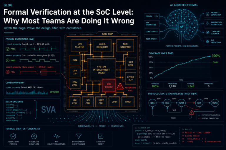
The Verification Crisis in Advanced Node Design As chip complexity doubles every technology generation, traditional verification approaches are hitting a wall. Simulation-based verification takes months,...
📅 April 7, 2026⏰ 2 min read
Free Newsletter
Stay sharp. Get Spec to Silicon.
Weekly intelligence on VLSI, AI for EDA, and chip careers. 20,000+ engineers already inside.